M100ROM: Difference between revisions
m (Add /CE jumper in place of lower diode.) |
|||
| (28 intermediate revisions by one other user not shown) | |||
| Line 6: | Line 6: | ||
== Supported Models == | == Supported Models == | ||
* Model 100 only | * Model 100 only | ||
* Note: when used with a 27C512 as an Option ROM device, this becomes incompatible with REX | |||
== | == About == | ||
[[Image:M100rom1.jpg]] | [[Image:M100rom1.jpg]] | ||
This is a DIY project; by getting all the parts, you can assemble this yourself without much effort. | |||
The M100ROM adapter has several (fixed at assembly time) options: | The M100ROM adapter has several (fixed at assembly time) options: | ||
1 - Just convert non-standard pinout to standard JEDEC, to use a 256Kb (32KB) (E)EPROM in an old M100. | 1 - Just convert non-standard pinout to standard JEDEC, to use a 256Kb (32KB) (E)EPROM in an old M100 (e.g. to update 19xx year to 20xx). | ||
2 - Same as #1, but using a 512Kb (64KB) (E)EPROM with an option ROM image in the upper half. | 2 - Same as #1, but using a 512Kb (64KB) (E)EPROM with an option ROM image in the upper half. | ||
3 - Same as #2, but without pinout conversion, for use in a 'new' M100. | 3 - Same as #2, but without pinout conversion, for use in a 'new' M100. | ||
If you have a 'new' M100 with the standard socket you can accomplish #3 with a simple 'shim' socket that goes between the system ROM socket and the EPROM and breaks the chip select connection, replacing it with a diode-and connection (with pull-up) to both the original system and the option ROM select signals and a connection to the '512's uppermost address line. The only added connection to the board is a clip lead to the ROM select at M5 pin 5. | If you have a 'new' M100 with the standard socket you can accomplish #3 with a simple 'shim' socket that goes between the system ROM socket and the EPROM and breaks the chip select connection, replacing it with a diode-and connection (with pull-up) to both the original system and the option ROM select signals and a connection to the '512's uppermost address line. The only added connection to the board is a clip lead to the ROM select at M5 pin 5. | ||
== How to Get One == | == How to Get One == | ||
You need the following parts- | |||
1x M100ROM PCB from Oshpark | |||
2x 1N4148 diode or equivalent | |||
1x 10K 1/8W or 1/4W leaded resistor | |||
1x 27C256 or 27C512 (pre-programmed ideally) | |||
28x pins for connecting the module to the M100 ROM socket | |||
== A bit about EEPROM Pinouts == | |||
The table below shows the standard pinouts for 27C256 and 27C512, included for reference. | |||
[[Image:eeproms.png]] | |||
== Assembly == | |||
Modifications for 27C256: | |||
Installation using 27C256 requires that the track between via CE1 and adjacent via IC1 be cut. | |||
Use a dremel tool or sharp hobby knife to remove the copper track. | |||
Assuming you did not install the diodes and resistor required for the 27C512 you will also need | |||
to add a jumper in place of the diode closest to the IC (between the labels '1N4148' and '/CE2') | |||
Although not necessarily required, add a jumper between the via 'Vcc' and adjacent 'IC-1' | |||
Steps: | |||
* pre-program your device; for 27C256, burn in your presumably updated image. For 27C512, burn in your updated main ROM image in the lower 32k, and program your Option ROM into the upper 32k. | |||
* if 27C256 is planned, cut track between via CE1 and adjacent via IC1; also see above. | |||
* solder your 28 pins to the PCB. Ensure you place the pins in the rows that make sense. For early M100 use the rows marked "OLD" and for late M100 that have the standard pinout, use "NEW". Lots of ways to do this, but keep in mind that the pins have to be very low profile. The board has to sit right on top of the socket for clearance. | |||
Solutions for pins include small gauge stripped wire, or if you can find them, some stake pins. | |||
If someone finds a good solution for pins, please post here. | |||
http://www.ebay.com/itm/50x-Batten-and-Allen-BA3760-Dill-Leadframe-DIP-PCB-Edge-Clip-Pins-BASIC-Stamp-/261518387239?pt=LH_DefaultDomain_0&hash=item3ce3b5e827 | |||
this is a good solution; you'd have to clip off the bottom, insert through the board into the socket, and solder from the top. Then, trim flush. | |||
* insert the IC in the row marked IC, and solder away. Ensure orientation is correct. | |||
* for 27C512, insert resistor and diodes where indicated, paying attention to orientation, and solder. | |||
== Board == | |||
The bare PCB can be ordered here: | |||
https://www.oshpark.com/shared_projects/Kil9S1ya | |||
Cost is 7.50$ USD for 3 boards. | |||
[[Image:pri.png]] | |||
[[Image:sec.png]] | |||
The copper for this board is shown here for wiring clarity. | |||
[[Image:pri_copper.png]] | |||
[[Image:sec_copper.png]] | |||
== Programming the EEPROM after assembly == | |||
If you did not pre-program the EEPROM, then you can do so after assembly with a little extra effort. | |||
The vias at the bottom are used to program the device after it is assembled. | |||
On a 27C256, to program the device you must tie pin 1 to Vpp. | |||
Ensure that the track between via CE1 and adjacent via IC1 is cut. | |||
Apply Vpp to either IC-1 via. | |||
On a 27C512, to program the device you must tie pin 22 to Vpp. | |||
No track cuts are required. | |||
Apply Vpp to PGM via. | |||
Of course you must have valid signals on the address and data lines, and you also have to apply 5V to Vcc via, and ground at socket pin 14. | |||
== Schematic == | |||
Schematic was lost unfortunately. However an earlier version, without the extra vias for programming the device after manufacture, is here. Note that the schematic shows the pinout for the 27C512, and pin 22 is also used as programming voltage. On the 27C256, programming voltage is on Pin 1, which in this case is connected to via marked CE1. | |||
[[Image:M100rom_schem.jpg]] | |||
== Installation == | |||
Installation of the hardware is a piece of cake. | |||
If you are interested only in a Main ROM replacement, then once completed the adapter should just plug in. | |||
If you are after an upgrade to Main ROM and also providing an OPTION ROM, then after you plug the module (and verify the machine boots normally), you need to run a wire from M5 pin 5 to the CE2 via. A good solution here is to solder a wire to CE2, and use a clip to connect to the IC pin. | |||
searching for "mini grabber" on ebay yields a solution for the clip. | |||
Latest revision as of 14:33, 4 July 2018
NEWS!
- Mike Stein has graciously released his board design through Oshpark so that people can get access to boards and build themselves a ROM adapter for Model 100!
Supported Models
- Model 100 only
- Note: when used with a 27C512 as an Option ROM device, this becomes incompatible with REX
About
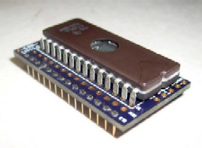
This is a DIY project; by getting all the parts, you can assemble this yourself without much effort. The M100ROM adapter has several (fixed at assembly time) options:
 1 - Just convert non-standard pinout to standard JEDEC, to use a 256Kb (32KB) (E)EPROM in an old M100 (e.g. to update 19xx year to 20xx).
 2 - Same as #1, but using a 512Kb (64KB) (E)EPROM with an option ROM image in the upper half.
 3 - Same as #2, but without pinout conversion, for use in a 'new' M100.
If you have a 'new' M100 with the standard socket you can accomplish #3 with a simple 'shim' socket that goes between the system ROM socket and the EPROM and breaks the chip select connection, replacing it with a diode-and connection (with pull-up) to both the original system and the option ROM select signals and a connection to the '512's uppermost address line. The only added connection to the board is a clip lead to the ROM select at M5 pin 5.
How to Get One
You need the following parts-
 1x M100ROM PCB from Oshpark
 2x 1N4148 diode or equivalent
 1x 10K 1/8W or 1/4W leaded resistor
 1x 27C256 or 27C512 (pre-programmed ideally)
 28x pins for connecting the module to the M100 ROM socket
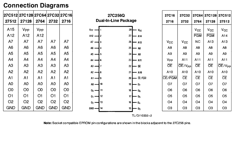
A bit about EEPROM Pinouts
The table below shows the standard pinouts for 27C256 and 27C512, included for reference.
Assembly
Modifications for 27C256:
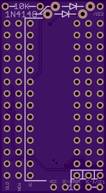
 Installation using 27C256 requires that the track between via CE1 and adjacent via IC1 be cut.
 Use a dremel tool or sharp hobby knife to remove the copper track.
 Assuming you did not install the diodes and resistor required for the 27C512 you will also need
 to add a jumper in place of the diode closest to the IC (between the labels '1N4148' and '/CE2')
Although not necessarily required, add a jumper between the via 'Vcc' and adjacent 'IC-1'
Steps:
- pre-program your device; for 27C256, burn in your presumably updated image. For 27C512, burn in your updated main ROM image in the lower 32k, and program your Option ROM into the upper 32k.
- if 27C256 is planned, cut track between via CE1 and adjacent via IC1; also see above.
- solder your 28 pins to the PCB. Ensure you place the pins in the rows that make sense. For early M100 use the rows marked "OLD" and for late M100 that have the standard pinout, use "NEW". Lots of ways to do this, but keep in mind that the pins have to be very low profile. The board has to sit right on top of the socket for clearance.
 Solutions for pins include small gauge stripped wire, or if you can find them, some stake pins.
 If someone finds a good solution for pins, please post here.
 http://www.ebay.com/itm/50x-Batten-and-Allen-BA3760-Dill-Leadframe-DIP-PCB-Edge-Clip-Pins-BASIC-Stamp-/261518387239?pt=LH_DefaultDomain_0&hash=item3ce3b5e827
 this is a good solution; you'd have to clip off the bottom, insert through the board into the socket, and solder from the top.  Then, trim flush.
- insert the IC in the row marked IC, and solder away. Ensure orientation is correct.
- for 27C512, insert resistor and diodes where indicated, paying attention to orientation, and solder.
Board
The bare PCB can be ordered here:
https://www.oshpark.com/shared_projects/Kil9S1ya
Cost is 7.50$ USD for 3 boards.
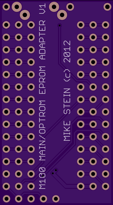
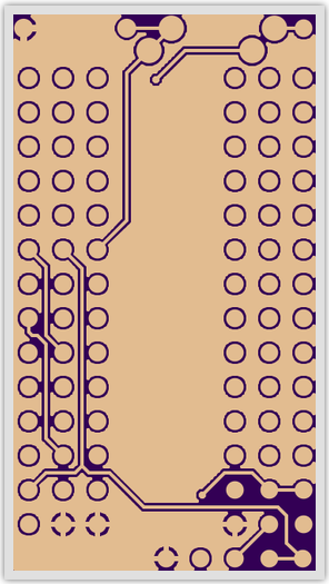
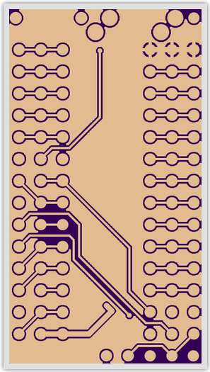
The copper for this board is shown here for wiring clarity.
Programming the EEPROM after assembly
If you did not pre-program the EEPROM, then you can do so after assembly with a little extra effort. The vias at the bottom are used to program the device after it is assembled.
 On a 27C256, to program the device you must tie pin 1 to Vpp.
 Ensure that the track between via CE1 and adjacent via IC1 is cut.
 Apply Vpp to either IC-1 via.
 On a 27C512, to program the device you must tie pin 22 to Vpp.
 No track cuts are required.
 Apply Vpp to PGM via.
Of course you must have valid signals on the address and data lines, and you also have to apply 5V to Vcc via, and ground at socket pin 14.
Schematic
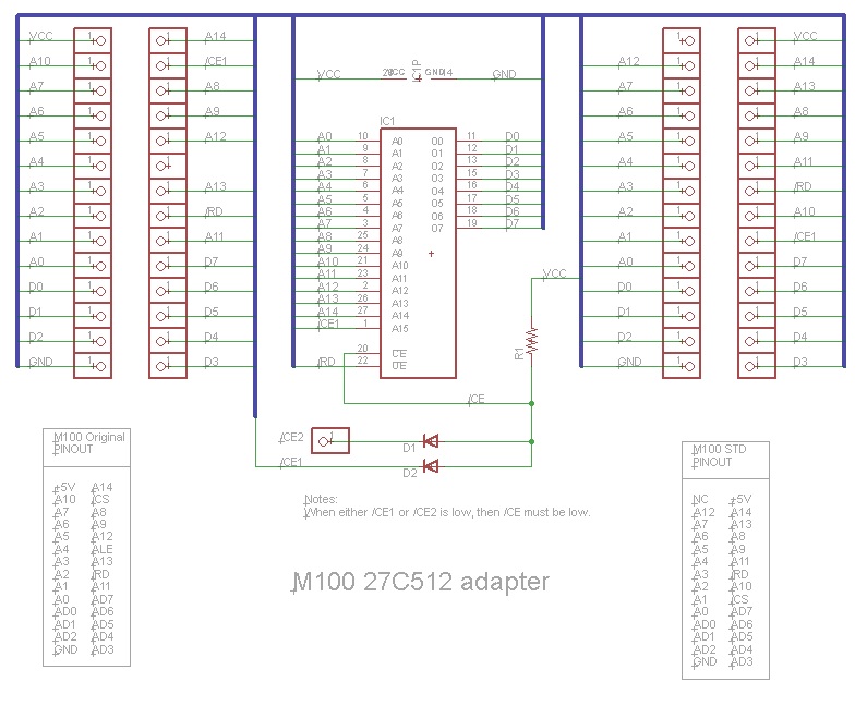
Schematic was lost unfortunately. However an earlier version, without the extra vias for programming the device after manufacture, is here. Note that the schematic shows the pinout for the 27C512, and pin 22 is also used as programming voltage. On the 27C256, programming voltage is on Pin 1, which in this case is connected to via marked CE1.
Installation
Installation of the hardware is a piece of cake. If you are interested only in a Main ROM replacement, then once completed the adapter should just plug in. If you are after an upgrade to Main ROM and also providing an OPTION ROM, then after you plug the module (and verify the machine boots normally), you need to run a wire from M5 pin 5 to the CE2 via. A good solution here is to solder a wire to CE2, and use a clip to connect to the IC pin.
searching for "mini grabber" on ebay yields a solution for the clip.
