5MHZ upgrade for Model T: Difference between revisions
| Line 34: | Line 34: | ||
|} | |} | ||
Since OSHPARK is so clumsy in dealing with PCB revisions (basically you can't remove a bad file design once shared), I've decided to just post PCB gerber files and schematics here. That way I can control issues that I find and always have the corrected files available. IF files are posted at OSHPark it won't be by me, so no promises. | |||
== Technical discussion == | == Technical discussion == | ||
Revision as of 14:02, 5 November 2023
Updated November 2023 work in progress
Goal of this page is to share the latest in a long sequence of "clock doubler" boards for the 80C85 used in the Model T computers.
Goals
  * support for all Model T computers - M100, T102, T200, PC-8201, PC-8300, M10, KC-85
  * buildable with moderate effort and skill
  * minimal and reversible modification to the computer
Features
  * software switchable speed up for compatibility
  * settable power-up default speed, 1x or 2x
  * hardware driven 1x slowdown function (needed for T200)
  * accelerated RAM timing signal (needed for M100, T102, NEC, KC-85, M10)
  * single sided component placement
  * 3 different crystal placement options for mechanical fit flexibility
  * surface mount logic, leaded through-hole passives
  * low power consumption
PCB and Schematic
| PCB | Version | Comments | Gerbers | Images | Schematic | Eagle design files |
| 1x 2x clock doubler | V4.4 | Includes all functions. | Gerbers V4_4 | Board images V4_4 | Schematic image V4_4 | Eagle design files V4_4 |
Since OSHPARK is so clumsy in dealing with PCB revisions (basically you can't remove a bad file design once shared), I've decided to just post PCB gerber files and schematics here. That way I can control issues that I find and always have the corrected files available. IF files are posted at OSHPark it won't be by me, so no promises.
Technical discussion
Power Consumption
In general, running at 5MHz consumes more power than 2.5MHz operation. In my experience, the speed increase tends to consume 15-20mA of power supply current.
In M100 for example, if the typical current is 56mA, 5MHz operation may drive up the current to 72mA or so.
My personal feeling is that it is much better to have the option to run fast than to worry about consuming more battery. To each their own.
M100
In the Model 100, running at 2x clock rate requires a solution to 2 issues in general.
  1.  The main ROM is typically too slow
  2.  The SRAM modules may also be too slow.
Either of these issues may impair operation at 5MHz. OR - you might get lucky and it runs fine as is.
Speeding up the Main ROM
In the M100 technical reference, there is a comment that states the main ROM has 600nsec timing. Original ROMs were this slow; newer ones were faster. If after installation and trial, you believe your main ROM is too slow, this can be easily overcome by swapping in an EPROM. There are several solutions for this - for example there are adapter boards that convert the custom M100 main ROM pinout to standard 27C256. I recommend using a 200nsec or faster EPROM. No need to change the binary image, but you can always convert to T102 ROM for the bug fixes.
Speeding up the SRAM
On early M100s the system RAM is also (barely) too slow. Early RAM modules were 250nsec SRAM. Take a look at your SRAM... if they are -25 then they are too slow. If they are -20 or -15, you are probably ok.
The original A* signal in the standard M100/T102 design, is used to minimize SRAM power by disabling the SRAM when no read/write is occurring. This is actually very important. The longer the SRAM stays "on" the more power it consumes. In a battery laptop, you want to shut of the SRAM as much as possible. However, the timing of the A* signal is quite delayed in the CPU read/write cycle. A* is driven by the /RD and /WR signals.
To make slow SRAM work at 5MHz, you need to create an A* signal that enables the SRAM a bit earlier in the CPU cycle. This special A* signal needs to be wired into the M100. This involves cutting one track and soldering one wire.
The clock doubler PCB includes a generation of a replacement A* signal, which allows the slower SRAM to work at 5MHz. As a result of the advanced A* timing, the power consumption goes up a little bit.
T102
T102 installation is very similar to the M100. I have not however observed any problem with Main ROM speed; it seems that the T102 benefits from being built later, and hence has faster main ROMs. T102 does however require modified A* timing just like the M100.
T200
T200 installation is simpler than M100/T102, in that there is no issue related to Main ROM or SRAM speed. But, T200 does have one gotcha. The real time clock chip RP5C01 is really slow and cannot run at 5MHz. Period. So, we need another solution.
The answer is to actually disable 5MHz operation when the CPU is accessing the real time clock chip. Thankfully, there is a pretty easy fix. The clock doubler PCB has a special input signal that, when low, disables 2x mode. Addition of a single wire to connect the "CL" signal at a specific location on the T200 motherboard, to this input allows the T200 to automatically slow down only when the RP5C01 is being selected.
NEC PC-8201
I have not yet done an actual install, but I expect it will have the same issues as M100.
  Expect the Main ROM may be slow, and needs a 27C256 upgrade.
  Expect there could be slow SRAM modules, and needs a new A* signal.
NEC PC-8300
I have not yet done an actual install, but I expect the machine is compatible with 5MHz operation with no problem with Main ROM or SRAM timing.
Olivetti M10
I have not yet done an actual install, but I expect it will have the same issues as M100.
  Expect the Main ROM may be slow, and needs a 27C256 upgrade.
  Expect there could be slow SRAM modules, and needs a new A* signal.
Kyocera KC-85
I have not yet done an actual install (because I don't have a KC-85!, but I expect it will have the same issues as M100.
  Expect the Main ROM may be slow, and needs a 27C256 upgrade.
  Expect there could be slow SRAM modules, and needs a new A* signal.
Software control of the clock doubler
To control the clock rate of the laptop, the following BASIC commands are used.
  OUT85,0   sets to 2.5MHz
  OUT85,1   sets to 5MHz
Easy to remember! 8085
Installation Files
| Computer model | Installation files |
| T102 | T102 1x/2x clk mod V1.0 Nov 2023.pdf |
| M100 | M100 1x/2x clk mod V1.0 Nov 2023.pdf |
| T200 | T200 1x/2x clk mod V1.0 Nov 2023.pdf |
| PC-8201 | not yet investigated |
| PC-8300 | not yet investigated |
| M10 | not yet investigated |
| KC-85 | like M100? |
As I test and more-or-less land on a reasonable upgrade process, I will post instruction files here If you have any questions, please get in touch with me at Twospruces at --the google mail service.
What are the tradeoffs?
A fixed solution makes your laptop always run at 5MHz. A switchable solution gives you the option of standard operation or "TURBO mode". The switchable solution is a nice way to go. Switch up when needed, switch down when necessary.
Some of the considerations are captured below.
Laptop functionality
| Item | Fixed 5MHz | Switchable 5MHz |
| Processor speed | 5MHz | 2.5 or 5 MHz |
| LCD | 5MHz | 2.5 or 5 MHz |
| I/O | 5MHz | 2.5 or 5 MHz |
| BCR | 5MHz | 2.5 or 5 MHz |
| Cassette | assumed non functional | functional in 2.5 MHz mode |
| Modem | standard | standard |
| Printer | standard | standard |
| Power consumption | ~40% higher | ~40% higher in 5MHz mode |
Complexity of modifications
| Item | Fixed 5MHz | Switchable 5MHz |
| Clock PCB assembly ease | easiest | small SMT soldering |
| Crystal location | swap onboard | mounted on adapter board |
| Clock PCB installation ease | easiest | additional wiring |
| M100 ROM upgrade | challenging to build | challenging to build |
| M100 main PCB cut tracks? | one clock trace | one clock trace |
| T102 main PCB cut tracks? | one clock trace and RAM mod | one clock trace and RAM mod |
| Reversible? | yes, remove hack and repair cut tracks | yes, remove hack and repair cut tracks |
What about compatibility with REX#/REXCPM?
REX# and REXCPM from November 2021 are built and tested compatible with 5MHz. In fact my test station runs at 5MHz. If you have an earlier REX#/REXCPM, contact me to discuss what to do.
Instructions
Take a look at the instruction files below. Please don't try this if you are not confident of success! I welcome feedback and comments. Especially if you find errors or improvements.
Fixed 5MHz Upgrades
| Computer model | Version | Upgrade file | Power consumption at 5MHz |
| T102 | Fixed 2x upgrade V1.2 | T102 5MHz mod V1.2 Apr2 2022.pdf | 80-100mA |
| M100 | Fixed 2x upgrade V1.1 | M100 5MHz mod V1.1 Apr 2022.pdf | 80-100mA |
| T102 | Fixed 2x upgrade V2.0 | T102 5MHz mod V2.0 .pdf | 65-75mA |
| M100 | Fixed 2x upgrade V2.0 | M100 5MHz mod V2.0 .pdf | 65-75mA |
Comments on these upgrades
Power consumption:
While effective, and simple, these two initial upgrade designs suffer from higher current than is desirable. Typical M100/T102 have power consumption in MENU of about 50 mA. I have observed that using these conversions, power can be between 80 and 100 mA. This seems to be due in part to how this conversion modifies the A* circuit.
Both of these initial conversions use a simple change to the A* circuit. Here the A* signal is tied to +5V, meaning the RAM is enabled quite early in the CPU cycle. While there is no conflict with this wiring, I now appreciate that there is an advantage to reducing the time over which the SRAM chips are enabled.
A* is used, in the standard design, to enable the SRAM only when there is an active READ or WRITE, driven by the /RD and /WR signals. This has the effect of turning the SRAM on for the minimum time duration.
SRAM has a fairly significant power draw when selected. So when the A* signal timing is modified (which is needed to support 5MHz operation), the longer the SRAM stays "on" the more power it consumes.
The good news is that I have a design that drops the RAM power significantly. I'll be posting that design shortly.
NSC800 / CP/M @ 5MHz
For M100 with NSC800, contact me for a solution. This would of course be a dedicated CP/M machine with REXCPM installed.
Switchable 5MHz Upgrades
| Computer model | Version | Upgrade file |
| T102 | Switchable 2x upgrade V1 | design is done. working on docs |
| M100 | Switchable 2x upgrade V1 | design is done. working on docs |
PCBs
Posted here so I can maintain and update the designs, are Gerber files and layout images.
| PCB | Version | Comments | Gerbers | Image |
| Fixed 5MHz clock board (/2 board) | This board has no small surface mount parts and uses main board crystal. Easiest! Does not include A* signal generation, so induces higher than ideal power consumption. | V2 | Divide by 2 PCB Gerbers | 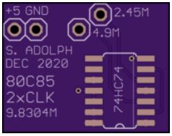
|
| Fixed 5MHz clock board (/2 board) + A* | This board has no small SMT and uses main board crystal. Includes A* generation to reduce power consumption to minimum. | V1 | Divide by 2 + A* PCB Gerbers | 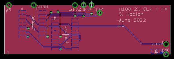
|
| Switchable 5MHz clock board + A* | Switchable design, with onboard crystal, timing generation and A* function. Harder to build, has small surface mount parts. | V4 | Switchable 2x/1x + A* PCB Gerbers | 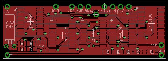
|
Photos
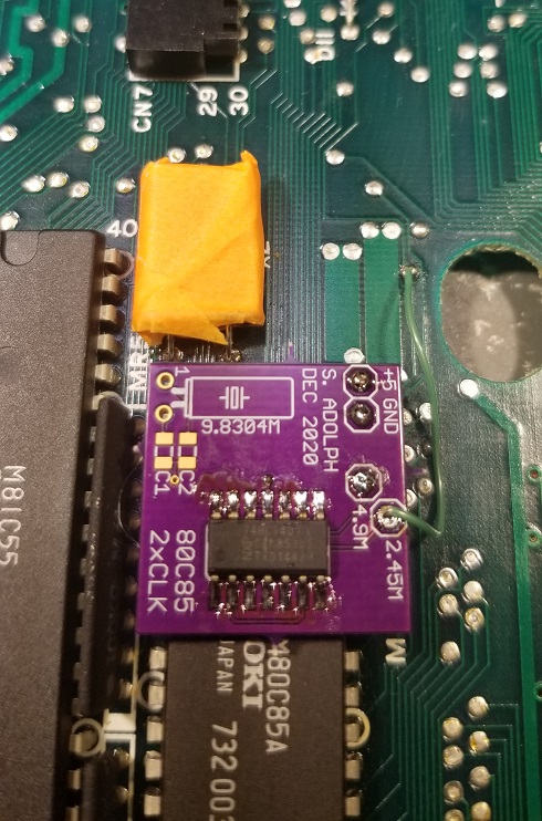
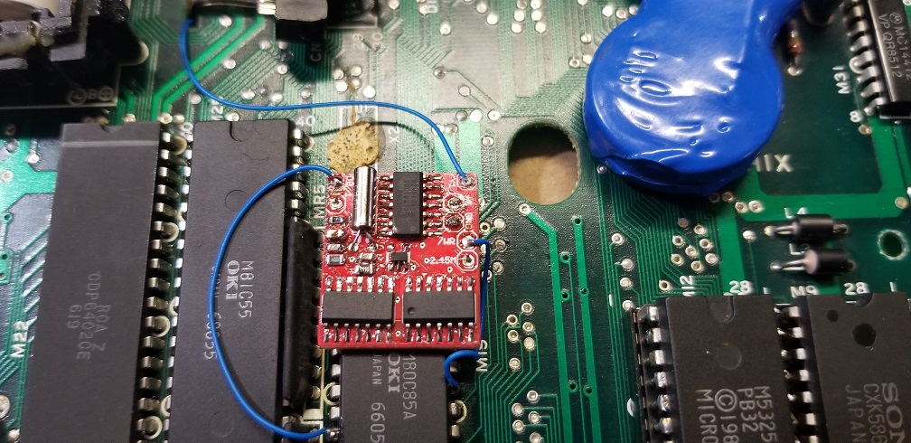
T102 with a fixed 5MHz board. This board is easy to make, and the 10M crystal is on the main board. No small SMT soldering! Note: what is shown is an early board. Latest board is more compact and eliminates the unused parts.
T102 with a switchable 5MHz board. This board has to use a crystal on the clock board, and has small SMT soldering. Harder to build, but has switchable clock.
This board is good, but there is a better solution.
FAQ
As this is tried I'm sure questions and comments will arise. We can capture useful information here. Thanks.
