NSC800 Conversion: Difference between revisions
No edit summary |
|||
| Line 37: | Line 37: | ||
== 1CPU NSC800 conversion PCB == | == 1CPU NSC800 conversion PCB == | ||
The current schematic is here. So far so good. May change. | |||
[[Media:1CPU_schem.PNG|1CPU_schem.PNG]] | |||
Layout is being optimized. Current layout is here as an example, but this board is not done yet. | |||
Gives you a sense for what's involved. | |||
[[Media:1CPU_pri.PNG|1CPU_pri.PNG]] | |||
[[Media:1CPU_sec.PNG|1CPU_sec.PNG]] | |||
Revision as of 08:21, 6 October 2020
Work in progress!
What is this all about?
Motivated by 2 things
- discovery (to me) of the NSC800 Z80 processor that is 80C85 like
- continuing to work in the direction of CP/M
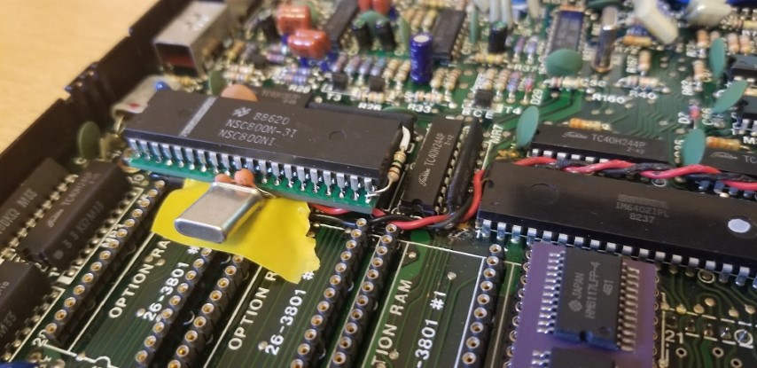
I have invested some time and effort in developing a conversion that supports NSC800 operation in the M100, both for standard BASIC use, as well as CP/M (in conjunction with REXCPM). Partly this has been motivated simply by curiosity. However, in CP/M it actually broadens the software applicability since quite a bit of CP/M software is Z80.
If you have an interested in doing this conversion please get in touch with me at Twospruces at --the google mail service.
There are 2 areas of change that are needed. Firstly you have to adapt the NSC800 to the 80C85 socket. There are a couple of tradeoffs to make. Secondly, the NSC800 needs to use a slightly different Main ROM.
To get started on this project, one can leverage the work done in the past. In fact an NSC800 conversion for 80C85 was posted back in the early 80s for S100 computers equipped with an 8080/8085 processor board. The information is posted below, from Microsystems September 1984.
This article lists considerations; from my work in M100 the things that any adapter has to deal with are listed below.
  1.  Inversion of the interrupt signals
  2.  Conversion of the 50/50 duty cycle RST7.5 signal to a 100 usec low pulse (NSC800 is level triggered not edge).
  3.  4.9152 MHZ clock generation circuitry.
  4.  And in the case of a dual processor conversion, certain NSC800 signals are not tri-state in RESET.
Note: it seems that the M100 RAM/ROM and REX are all tolerant of the short opcode fetch read/write cycle. So, no wait state generator appears to be needed.
While I have implemented both a DUAL 80C85/NSC800 CPU adapter, and a SINGLE NSC800 CPU conversion, I prefer the single conversion for it's simplicity.
1CPU NSC800 conversion PCB
The current schematic is here. So far so good. May change.
Layout is being optimized. Current layout is here as an example, but this board is not done yet. Gives you a sense for what's involved.
Modified M100 Main ROM
As mentioned, since the interrupt control mechanisms in NSC800 are slightly different, the M100 main ROM needs to be patched to support NSC800.
The NSC800 patch needs extra code space to be created in the ROM. To do that, an original patch has been verified that creates a block of unused space in the main ROM as published by Microsoft.
Once this base patch is applied to the ROM, you have space now for the next set of patches, here.
All these patches rolled up into a binary: (here I used the T102 base ROM as the starting point)
These are what I use today. If I find bugs I will post updates.
